
Unlock graphene’s atomic superpowers with pristine MOCVD direct-growth graphene.
For a decade, the commercialisation of graphene has been bottlenecked by the metal substrate "transfer" process. Paragraf has solved the problem.
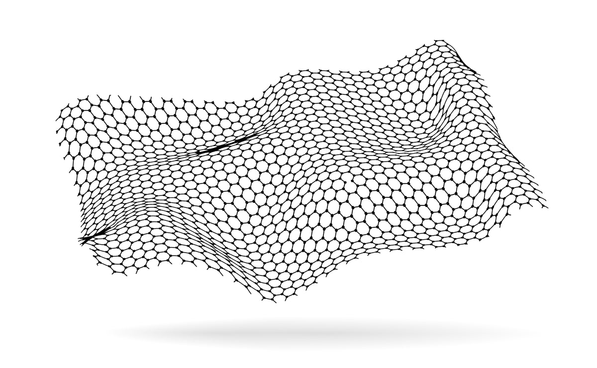
The Problem with Legacy CVD

Traditional Chemical Vapor Deposition (CVD) grows graphene on copper foil. To use it, the graphene must first be coated in a polymer support layer, typically PMMA. The copper substrate is then removed using acid etching before the graphene is physically transferred onto a semiconductor wafer.
Residual copper atoms, trapped polymer contamination, wrinkles and micro-fractures can remain within the material. The result is a graphene layer that varies from device to device, creating challenges for repeatability, yield and industrial scalability.
The Paragraf Breakthrough: Direct-Growth MOCVD

Paragraf's proprietary Metal-Organic Chemical Vapor Deposition (MOCVD) process grows graphene directly onto the final semiconductor substrate, typically 6-inch silicon or sapphire wafers. No copper or other metals.
Absence of a D-Peak
Raman spectroscopy demonstrates a high-quality graphene lattice, helping to preserve the intrinsic electrical and mechanical properties of the material.
Wafer-Scale Uniformity
Lot-to-lot baseline uniformity enables consistent production across millions of devices, enabling true CMOS foundry compatibility.
The Ultimate Blank Canvas
For molecular detection applications, MOCVD graphene provides a pristine surface for precise and repeatable functionalisation.